Nanohub.org ☑ energy band diagram pn junction forward bias Semiconductor junction schottky electron function affinity fermi parameters conduction
Prasanna's blog for electronics: Energy - band theory of solids
Energy band solids interatomic theory spacing crystal prasanna electronics fig Solved energy band diagram of a si p-n junction diode is Band diagram energy diode junction si below given help
Semiconductor nanohub fundamentals pause prev
Energy-band diagram for the metal-semiconductor junction (schottkyPrasanna's blog for electronics: energy Energy bandsEnergy bands semiconductors conductors insulators band gap based forbidden diagram theory definition formed classification physics size.
Pn junction biasEnergy band insulator diagram conductor semiconductor also revolution electrical Energy band diagaram ( conductor, semiconductor and insulator.


...

...

...

...
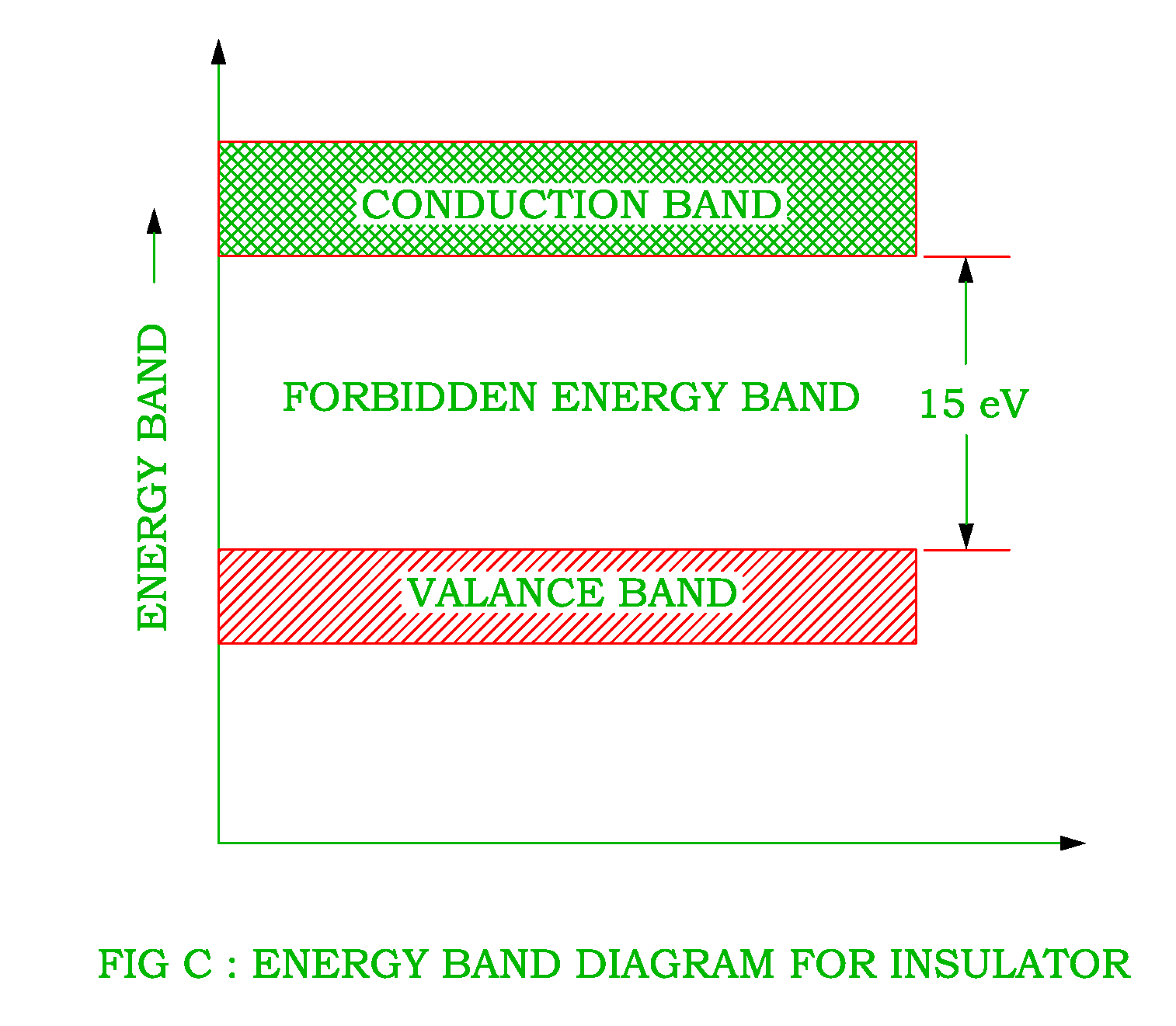
Energy Band Diagaram ( Conductor, Semiconductor and Insulator

...

...

☑ Energy Band Diagram Pn Junction Forward Bias

...

Solved Energy band diagram of a si p-n junction diode is | Chegg.com

Prasanna's blog for electronics: Energy - band theory of solids

